- 您现在的位置:买卖IC网 > Sheet目录478 > MMA20312BT1 (Freescale Semiconductor)IC AMP HBT INGAP/GAAS 12-QFN
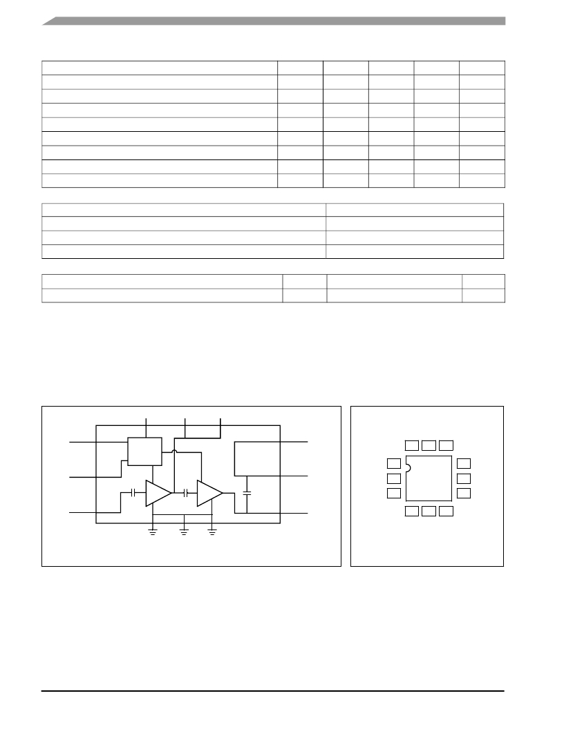
Table 4. Electrical Characteristics (V CC1 = V CC2 = V BIAS = 5 Vdc, 2140 MHz, T A = 25 ° C, 50 ohm system, in Freescale W--CDMA
Application Circuit)
Characteristic
Small--Signal Gain (S21) (1)
Input Return Loss (S11)
Output Return Loss (S22)
Power Output @ 1dB Compression, CW
Third Order Output Intercept Point, Two--Tone CW
Noise Figure
Supply Current (1,2)
Supply Voltage (2)
Symbol
G p
IRL
ORL
P1dB
OIP3
NF
I CQ
V CC
Min
23.6
—
—
—
—
—
62.5
—
Typ
27.2
--10.7
--15.5
28.2
44.5
3.3
70
5
Max
—
—
—
—
—
—
77
—
Unit
dB
dB
dB
dBm
dBm
dB
mA
V
Table 5. ESD Protection Characteristics
Test Methodology
Human Body Model (per JESD22--A114)
Machine Model (per EIA/JESD22--A115)
Charge Device Model (per JESD22--C101)
Table 6. Moisture Sensitivity Level
Class
0, rated to 150 V
A
III
Test Methodology
Per JESD22--A113, IPC/JEDEC J--STD--020
Rating
3
Package Peak Temperature
260
Unit
° C
1. Specified data is based on performance of soldered down part in W--CDMA application circuit.
2. For reliable operation, the junction temperature should not exceed 150 ° C.
V BA2
V CC1
V CC1
V BA1
BIAS
RF out
V BA2 V CC1 V CC1
12 11 10
CIRCUIT
V BA1
1
9
RF out
V BIAS
RF out
V BIAS
RF in
2
3
8
7
RF out
V CC2
RF in
V CC2
4 5 6
GND GND GND
GND
GND
GND
MMA20312BT1
2
Figure 1. Functional Block Diagram
Figure 2. Pin Connections
RF Device Data
Freescale Semiconductor, Inc.
发布紧急采购,3分钟左右您将得到回复。
相关PDF资料
MMA20312BVT1
IC AMP HBT INGAP/GAAS 12QFN
MMA2260DR2
IC ACCELEROMETER 16-SOIC
MMA3202KEGR2
SENSOR ACCEL +/-100/50G 20-SOIC
MMA5248WR2
IC ACCELER 480G X-AXIS 16QFN
MMA6331LT
SENSORS ACCELEROMETER 14LGA
MMA6341LT
IC ACCELER 3G/8G XY-AXIS 14LGA
MMA6361LT
IC ACCELER 1.5G XY-AXIS 14LGA
MMA6527KW
IC ACCELEROMETER XY AXIS 16QFN
相关代理商/技术参数
MMA20312BV
制造商:FREESCALE 制造商全称:Freescale Semiconductor, Inc 功能描述:Heterojunction Bipolar Transistor Technology
MMA20312BVT1
功能描述:射频GaAs晶体管 31dBm GaAs PA3-5V 3X3-12 RoHS:否 制造商:TriQuint Semiconductor 技术类型:pHEMT 频率:500 MHz to 3 GHz 增益:10 dB 噪声系数: 正向跨导 gFS(最大值/最小值):4 S 漏源电压 VDS: 闸/源击穿电压:- 8 V 漏极连续电流:3 A 最大工作温度:+ 150 C 功率耗散:10 W 安装风格: 封装 / 箱体:
MMA20LE1084GA
制造商:PARA LIGHT 功能描述:5x7 Blue Dot Matrix LED Display 制造商:Para Light Corp 功能描述:5x7 Blue Dot Matrix LED Display
MMA21-005
功能描述:CONN RACK/PANEL 5POS 5A RoHS:否 类别:连接器,互连式 >> 背板 - 专用 系列:MM22 标准包装:44 系列:PwrBlade® 连接器用途:- 连接器类型:插座,母插口和片状插口 连接器类型:叶片形电源 位置数:26 加载位置的数目:全部 间距:0.100"(2.54mm) 行数:4 列数:- 安装类型:板边缘,通孔,直角 端子:焊接 触点布局,典型:24 信号,2 电源 特点:导向引脚 触点表面涂层:金 触点涂层厚度:30µin(0.76µm) 颜色:黑 包装:托盘 额定电流:- 材料可燃性额定值:UL94 V-0 工作温度:-20°C ~ 105°C 额定电压:-
MMA21-0051A1
功能描述:CONN RACK/PANEL 5POS 5A RoHS:否 类别:连接器,互连式 >> 背板 - 专用 系列:MM22 标准包装:8 系列:PwrBlade® 连接器用途:- 连接器类型:插座,母插口和片状插口 连接器类型:叶片形电源 位置数:37 加载位置的数目:全部 间距:0.100"(2.54mm) 行数:4 列数:- 安装类型:板边缘,通孔,直角 端子:焊接 触点布局,典型:24 信号,13 电源 特点:板锁,导向引脚 触点表面涂层:金 触点涂层厚度:30µin(0.76µm) 颜色:黑 包装:托盘 额定电流:- 材料可燃性额定值:UL94 V-0 工作温度:-20°C ~ 105°C 额定电压:- 其它名称:51793-151793-1-ND
MMA21-0051C1
功能描述:CONN RACK/PANEL 5POS 5A RoHS:否 类别:连接器,互连式 >> 背板 - 专用 系列:MM22 标准包装:8 系列:PwrBlade® 连接器用途:- 连接器类型:插座,母插口和片状插口 连接器类型:叶片形电源 位置数:37 加载位置的数目:全部 间距:0.100"(2.54mm) 行数:4 列数:- 安装类型:板边缘,通孔,直角 端子:焊接 触点布局,典型:24 信号,13 电源 特点:板锁,导向引脚 触点表面涂层:金 触点涂层厚度:30µin(0.76µm) 颜色:黑 包装:托盘 额定电流:- 材料可燃性额定值:UL94 V-0 工作温度:-20°C ~ 105°C 额定电压:- 其它名称:51793-151793-1-ND
MMA21-0051D1
功能描述:CONN RACK/PANEL 5POS 5A RoHS:否 类别:连接器,互连式 >> 背板 - 专用 系列:MM22 标准包装:8 系列:PwrBlade® 连接器用途:- 连接器类型:插座,母插口和片状插口 连接器类型:叶片形电源 位置数:37 加载位置的数目:全部 间距:0.100"(2.54mm) 行数:4 列数:- 安装类型:板边缘,通孔,直角 端子:焊接 触点布局,典型:24 信号,13 电源 特点:板锁,导向引脚 触点表面涂层:金 触点涂层厚度:30µin(0.76µm) 颜色:黑 包装:托盘 额定电流:- 材料可燃性额定值:UL94 V-0 工作温度:-20°C ~ 105°C 额定电压:- 其它名称:51793-151793-1-ND
MMA21-0051H1
功能描述:机架和面板连接器 RACK & PANEL CONNECTOR RoHS:否 制造商:AVX 系列: 产品类型: 位置/触点数量: 安装风格: 端接类型: 外壳材料: 触点材料: 触点电镀:
